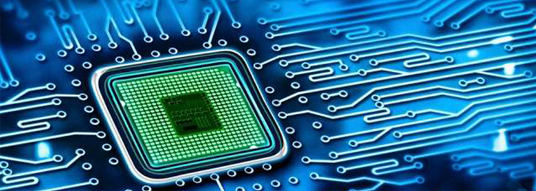
VLSI Technology
Very large-scale integration is a process of embedding or integrating hundreds of thousands of transistors onto a singular silicon semiconductor microchip. VLSI technology's conception dates back to the late 1970s when advanced level processor (computer) microchips were also in their development stages. Two of the most common VLSI devices are the microprocessor and the microcontroller.
VLSI refers to an integrated circuit technology with numerous devices on a single chip. The term originates, of course, in the 1970s, along with various other scale integration classifications based on the number of gates or transistors per IC.
The remarkable growth of the electronics industry is primarily due to the advances in large-scale integration technologies. With the arrival of VLSI designs, the number of possibilities for ICs in control applications, telecommunications, high-performance computing, and consumer electronics as a whole continues to rise.
Presently, technologies like smartphones and cellular communications afford unprecedented portability, processing capabilities, and application access due to VLSI technology. The forecast for this trend indicates a rapid increase as demands continue to increase.
The Advantages of VLSI Technology
The following are the primary advantages of VLSI technology:
Reduced size for circuits
- Increased cost-effectiveness for devices
- Improved performance in terms of the operating speed of circuits
- Requires less power than discrete components
- Higher device reliability
- Requires less space and promotes miniaturization
The Design Process of a VLSI IC
Overall, VLSI IC design incorporates two primary stages or parts:
1. Front-End Design:
This includes digital design using a hardware description language, for example, Verilog, System Verilog, and VHDL. Furthermore, this stage encompasses design verification via simulation and other verification techniques. The entire process also incorporates designing, which starts with the gates and continues through to design for testability.
2. Back-End Design:
This consists of characterization and CMOS library design. Additionally, it involves fault simulation and physical design.
The entire design process follows a step-by-step approach, and the following are the front-end design steps:
- Problem Specification: This is a high-level interpretation of a system. We address the key parameters, such as design techniques, functionality, performance, fabrication technology, and physical dimensions. The final specifications include the power, functionality, speed, and size of the VLSI system.
- Architecture Definition: This includes fundamental specifications such as floating-point units and which system to use, such as RISC or CISC and ALU's cache size.
- Functional Design: This recognizes the vital functional units of a system and, thus, enables identification of each unit’s physical and electrical specifications and interconnects requirements.
- Logic Design: This step involves control flow, Boolean expressions, word width, and register allocation.
- Circuit Design: This step performs the realization of the circuit in the form of a netlist. Since this is a software step, it utilizes simulation to check the outcome.
- Physical Design: In this step, we create the layout by converting the netlist into a geometrical depiction. This step also follows some preconceived static rules, such as the lambda rules, which afford precise details of the ratio, spacing between components, and size.
The following are the back-end design steps for hardware development:
- Wafer Processing: This step utilizes pure silicon melted in a pot at 1400º C. Then, a small seed comprising the required crystal orientation is injected into liquefied silicon and gradually pulled out, 1mm per minute. We manufacture the silicon crystal as a cylindrical ingot and cut it into discs or wafers before polishing and crystal orientation.
- Lithography: This process (photolithography) includes masking with photo etching and a photographic mask. Next, we apply a photoresist film on the wafer. A photo aligner then aligns the wafer to a mask. Finally, we expose the wafer to ultraviolet light, thus highlighting the tracks through the mask.
- Etching: Here, we selectively remove material from the surface of the wafer to produce patterns. With an etching mask to protect the essential parts of the material, we use additional plasma or chemicals to remove the remaining photoresist.
- Ion Implantation: Here, we utilize a method to achieve a desired electrical characteristic in the semiconductor, i.e., a process of adding dopants. The process uses a beam of high-energy dopant ions to target precise areas of the wafer. The beam's energy level determines the depth of wafer penetration.
Metallization: In this step, we apply a thin layer of aluminum over the entire wafer.
Assembly and Packaging: Every one of the wafers contains hundreds of chips. Therefore, we use a diamond saw to cut the wafers into single chips. Afterward, they receive electrical testing, and we discard the failures. In contrast, those that pass receive a thorough visual inspection utilizing a microscope. Finally, we package the chips that pass the visual inspection as well as recheck them.
VLSI technology is ideally suited to the demands of today's electronic devices and systems. With the ever-increasing demand for miniaturization, portability, performance, reliability, and functionality, VLSI technology will continue to drive electronics advancement.